
The Hardware Behind Dopre
Introducing Dopre, a method to use QMK on custom electrostatic capacitive (Topre, NiZ) keyboards. Dopre is a fully custom solution that requires the implementation of new PCBs. Dopre is not suitable for adapting existing PCBs to QMK.
Dopre is heavily influenced by Tom Smalley’s Custom Topre Guide.
What Is Electrostatic Capacitive?
You may or may not be familiar with electrostatic capacitive (ESC) keyboards before reading this page. If not, don’t worry.
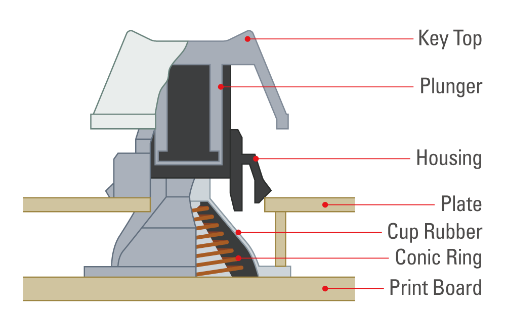
Simply put, it’s a type of keyswitch that works by pressing down on a silicone dome, that collapses on a conical spring. Unlike a traditional mechanical switch, this spring doesn’t define the force curve of the key. Instead, the dome is what is what provides feedback to the user.
You’ll commonly see ESC domes referred to as “rubber,” even in this diagram. However these domes are made of silicone, as noted in the description of some replacement domes1.
How It Works
An ESC switch uses a variable capacitance to sense whether or not a key has been pressed2. For comparison, a traditional mechanical keyswitch (Cherry, Kailh, etc.) simply completes a digital circuit when pressed3. As long as a mechanical keyswitch is pressed passed its “actuation” point, the connection will be made and the key will be registered as pressed.
Following this example, an ESC switch is always “on,” by the mechanical keyswitch logic. The signal sent to the switch always makes its way through the switch’s footprint on the PCB and the circuit is never broken by the switch. This means that an ESC switch works a bit differently than a mechanical one. It imparts an amount of capacitance on this connection. A typical digital GPIO connection would completely ignore this capacitance and only read the voltage. Therefore, an ESC keyboard must use some means of sensing this capacitance. Unfortunately for us, this is easier said than done.
How is Capacitance Generated?
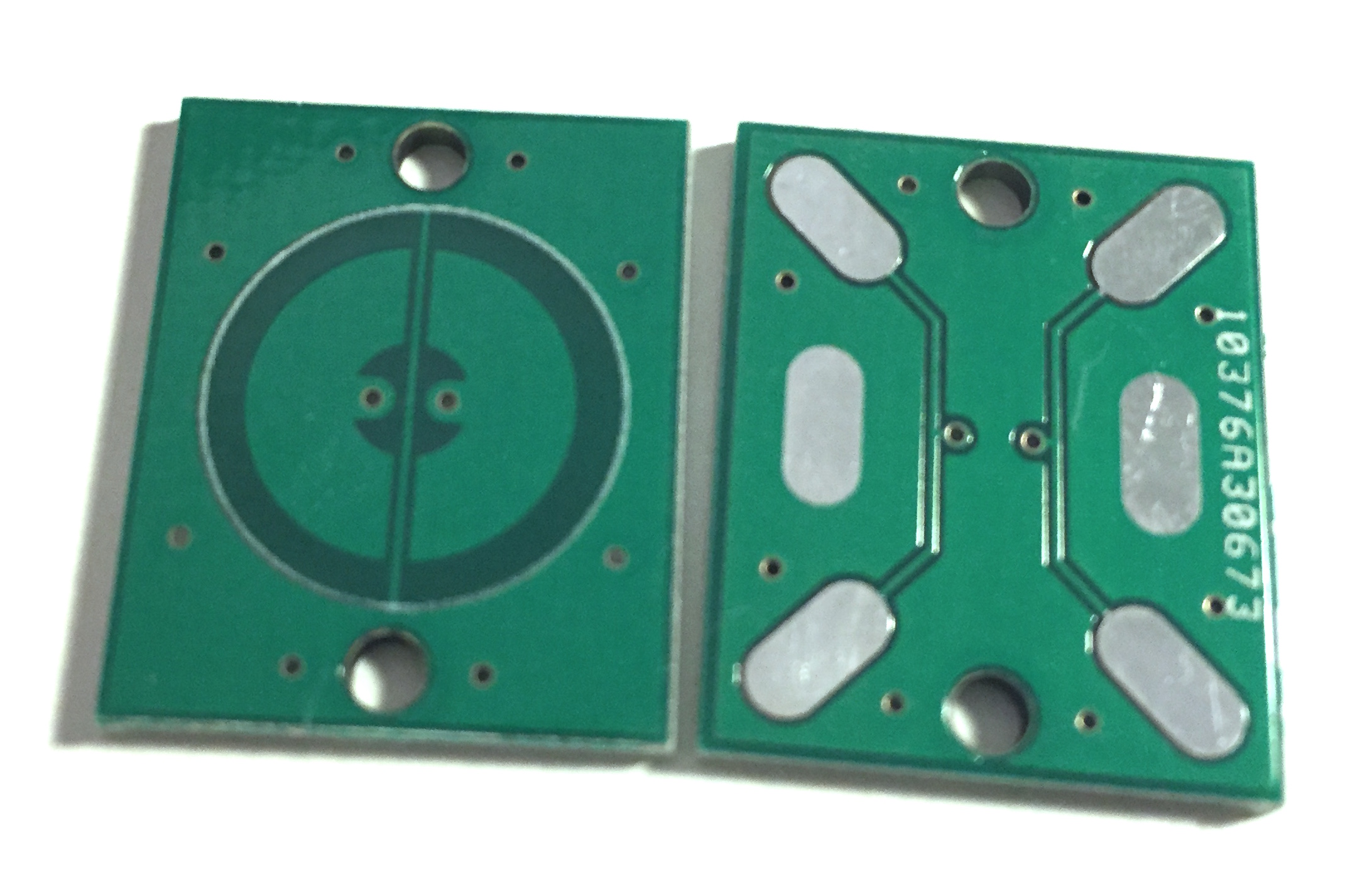
The trick to generating capacitance is the “conic ring,” or conical spring. This spring is specifically designed to act as a capacitor and will generate a larger capacitance as it is compressed. Capacitors work by having two metal plates that stay very close to each other, but do not touch. This allows a charge to be stored in the magnetic fields between these two pieces of metal. So if you reference the picture of an ESC pad in this section, you’ll notice there are two half-circles separated by a trace. The signal is sent into one half of this circle, and the spring acts as a means to transfer that signal on to the other half of the circle. As more of the spring is depressed, there is more surface area to build up a larger magnetic field, and thus a larger capacitance.
This spring generates a capacitance somewhere between 0 and 6 picofarads, depending on how far it is compressed2. Thankfully for us, the conical shape of the spring actually gives us an advantage here. This cone shape actually means that the capacitance increases linearly, as the switch is pressed. This means that we can get a full range of accurate readings for every level of key depression.
Why Use Electrostatic Capacitive
There are a couple reasons that you might want to use an ESC keyboard4, but they might all just be marketing hype. Try one out for yourself to see what you think of it compared to a traditional mechanical keyswitch.
Here are a couple of notable reasons you may be interested in an ESC keyboard:
-
Customizable actuation points - A traditional mechanical keyswitch will always actuate at the same point. However, an ESC switch can have its actuation point moved lower or higher. This is often advertised as a “gaming” feature to make your key presses record faster, but this is probably all marketing hype. It could, however, be used to help soft typists that don’t fully press keys. Or for those of us who do bottom out our keys, it could help train us to stop doing so by actuating earlier.
-
Key feel - The experience of using a Topre switch is markedly different from using a mechanical switch. Most importantly, when you fully depress a key, the bottom out experience is much softer. This can be a major boon that suffer from pain when typing for long periods.
How to Sense Capacitance
Believe it or not, capacitance sensing is actually some pretty well-worn territory. If you’ve used the PS4, the Xbox One, or a variety of other electronics, you might be familiar with those buttons that aren’t really buttons. You know the ones that your pets activate just by brushing by them. These fake-buttons are capacitive buttons. They run a tiny voltage through a pad that senses when your hand (or your dog) gets near to them. This change in capacitance can be considered a “touch” and is interpreted as a button press. Texas Instruments actually has a guide that covers that basics of capacitive sensing, if you are looking for further information.
You’re probably also very familiar with capacitance sensing solutions seeing as pretty much every phone and tablet these days uses capacitance sensing to determine when and how you are touching the screen5. Its been the de-facto standard for quite some time now, beating out the old resistive technology. You may also remember resistive touch from old PDAs or even the big Wii U tablet. Suffice to say that capacitance sensing beat out resistive solutions for a good reason.
Initial Concerns
There are two main issues we need to worry about when evaluating a method to sense capacitance.
- Speed
- Resolution
Speed
First up, speed. USB polls devices at 125 Hz, but is adjustable up to 1000 Hz6. Ideally, we would want to be able to check every switch in that time window. For a full size keyboard at 1000 Hz, we would need 104 samples per millisecond, or 104 kilosamples per second. This equates to a frequency of 104 kHz (0.104 MHz). You’ll find that most traditional mechanical keyboards are not scanned in their entirety that fast, at least not ones flashed with QMK. Comparatively, if we wanted to scan the full keyboard at the standard 125 Hz, we have 8 times the available time per switch. Meaning that we’d need to sample at 13 kilosamples per second, or 13 kHz. This is a much more attainable number.
Let’s say that 13kHz may not be attainable, so what’s our minimum viable latency? Older studies posit that anything faster than 100 ms is considered instantaneous to a user, but if modern gaming has taught us anything, it’s that modern standards require something a bit faster than that7. Let’s consider 50 and 13 milliseconds of latency as our bare minimum response time, and see how this all stacks up alongside some frequencies you may be familiar with.
| Latency | Frequency (board) | Frequency (key, 100%) | Key Latency |
|---|---|---|---|
| 4 ms | 240 Hz | 24,960 Hz (25.0 kHz) | 40 uS |
| 7 ms | 144 Hz | 14,976 Hz (15.0 kHz) | 67 uS |
| 8 ms | 120 Hz | 12,480 Hz (12.5 kHz) | 80 uS |
| 13 ms | 77 Hz | 8,008 Hz (8.0 kHz) | 130 uS |
| 16 ms | 60 Hz | 6,240 Hz (6.2 kHz) | 160 uS |
| 33 ms | 30 Hz | 3,120 Hz (3.1 kHz) | 320 uS |
| 50 ms | 20 Hz | 2,080 Hz (2.1 kHz) | 480 US |
For this example, we are using a 104 key keyboard to determine our key latency. These numbers might be confusing, so lets explain them. Our latency is the maximum amount of time that can be devoted to scanning a whole keyboard. We need to scan every key once every “latency” time period to stay below this latency. Our board frequency is how often we would need to scan the whole board in order to maintain an update rate faster than this latency. It is a simple calculation using our latency as the period of our frequency. Our key frequency is our board frequency times the number of keys on the keyboard. In our case, that’s 104. This represents how many keys we would need to scan per second to reach our target board latency. We then go into key latencies, which are the maximum amount of time that can elapse between scanning two consecutive keys in order to meet our target latency and frequency.
A full sized keyboard is used to consider a “worst case” scenario for minimum viability. However, it is worth mentioning that smaller keyboards will operate with lower latencies because they have less keys to scan, and can therefore devote more time to each key.
So to sum up our findings, if our solution resolves the value of one key every 200 microseconds, we should have a fairly good latency on our board.
Resolution
Resolution is pretty straightforward, but worth mentioning. For one, we have to make sure that the entirety of our 0-6 pF range doesn’t disappear entirely. So if the resolution of our system is > 6 pF, that’s an obvious no-go. Our resolution will need to be 1 pF at least, with the actual value ideally being somewhere around 90 fF.
Using Something Off-The-Shelf
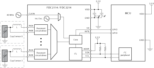
While Texas Instruments offers some pretty awesome capacitive sensing solutions, they are a little bit overbuilt for our cases. We’ll use them as an example to cover the application of general-purpose capacitive sensing solutions to the ESC switch problem. All of the details I am going to discuss are covered in the FDC2114 data sheet.
Off-The-Shelf Resolution
If we look at the details given to us as part of this datasheet, we can find that the maximum capacitance that can be read is 250 nanofarads at 10 kilohertz with a 1 millihenry inductor. That’s all fine and good, as 6 picofarads is way smaller than that. We can also note that the noise floor is at 0.3 femtofarads. This is also great as it’s way lower than anything we’d ever care about. So that means that we’d have a range of (roughly) 0 to 250 nanofarads. If we do some math, we end up with these resolutions:
| Chip | Bits | Max Reading | Math | Resolution |
|---|---|---|---|---|
| FDC221X | 28 | (2^28) 268,435,456 | 250 nF / (2^28) | 0.9313 fF |
| FDC211X | 12 | (2^12) 4,096 | 250 nF / (2^12) | 61.04 pF |
So right off the bat, we have a problem with the FDC211X series of chips. Notably, the resolution of the chip makes our 6 pF difference disappear into a single value. So we lose all accuracy with that one. However, the resolution of the FDC221X looks great. This would mean that our application would cover all readings from 0 to 6442, or the first 13 bits of our result.
Off-The-Shelf Speed
The problems start to arise when we talk about the the sample rate. The FDC211X has an outstanding sample rate of 13.3 kilosamples per second, whereas the FDC221X has a much less astonishing 4.08 kilosamples per second. If you reference the scan speed concerns section of this document, you’ll see that 4.08 ksps will put us into “acceptable” resolution territory, whereas 13.3 ksps would let us scan a whole board faster than a 120 Hz monitor could refresh.
Trying to Solve Our Problems
So where does that leave us? The FCD221X is too slow, and the FDC211X isn’t accurate enough. So can we play with these devices to try and solve our problems? We sure can give a shot.
You may remember that the maximum input capacitance that we have been using was qualified with a frequency and inductor. By varying the value of this inductor, we can adjust our maximum input capacitance reading and adjust our sample rate. By adjusting our maximum down with a different inductor, we might be able to get a reasonable resolution out of this chip.
Further Investigation in Off-The-Shelf
Given the increasing complexity of implementation of an Off-The-Shelf solution, the fact that the Off-The-Shelf solution uses 3V logic (requiring ARM or conversion circuitry), in conjunction with the fact that QMK still doesn’t have full I2C support for ARM devices at time of writing, this solution was shelved, pending further research.
The datasheet for the FDC2X1X devices talks about something called “differential sensor configuration.” All of the development boards opt for the “single-ended sensor configuration,” but the differential configuration is explicitly designed for a pad that works as a variable capacitor, which is exactly what we are doing. This implementation also needs to be explored.
The biggest notable advantage of the Off-The-Shelf solution is that is would provide a normalized value across the full range of an ESC switch. This would make ESC switches suitable to be used as analog inputs for purposes like emulating game joysticks. That application is considered outside the scope of Dopre, but it is certainly worth investigating.
Using an RC Circuit
First off, what is an RC circuit? It’s a circuit that slowly charges and discharges over time, notably named for being a circuit that contains a resistor (R) and capacitor (C)8. This is important because the rate and level of charge are proportional to the resistance and capacitance of the circuit used. This means that we can convert our variable capacitance into a variable voltage. Modern microcontrollers and pretty much all equipped with an analog to digital converter (ADC) that we can use to convert this voltage into a digital value to use in our software.
Now we’ll dig in to the details. Note that much of the content of this section comes from Tom Smalley’s Custom Topre Guide. So if you’ve read that guide before, you will likely see a lot of repeated content here.
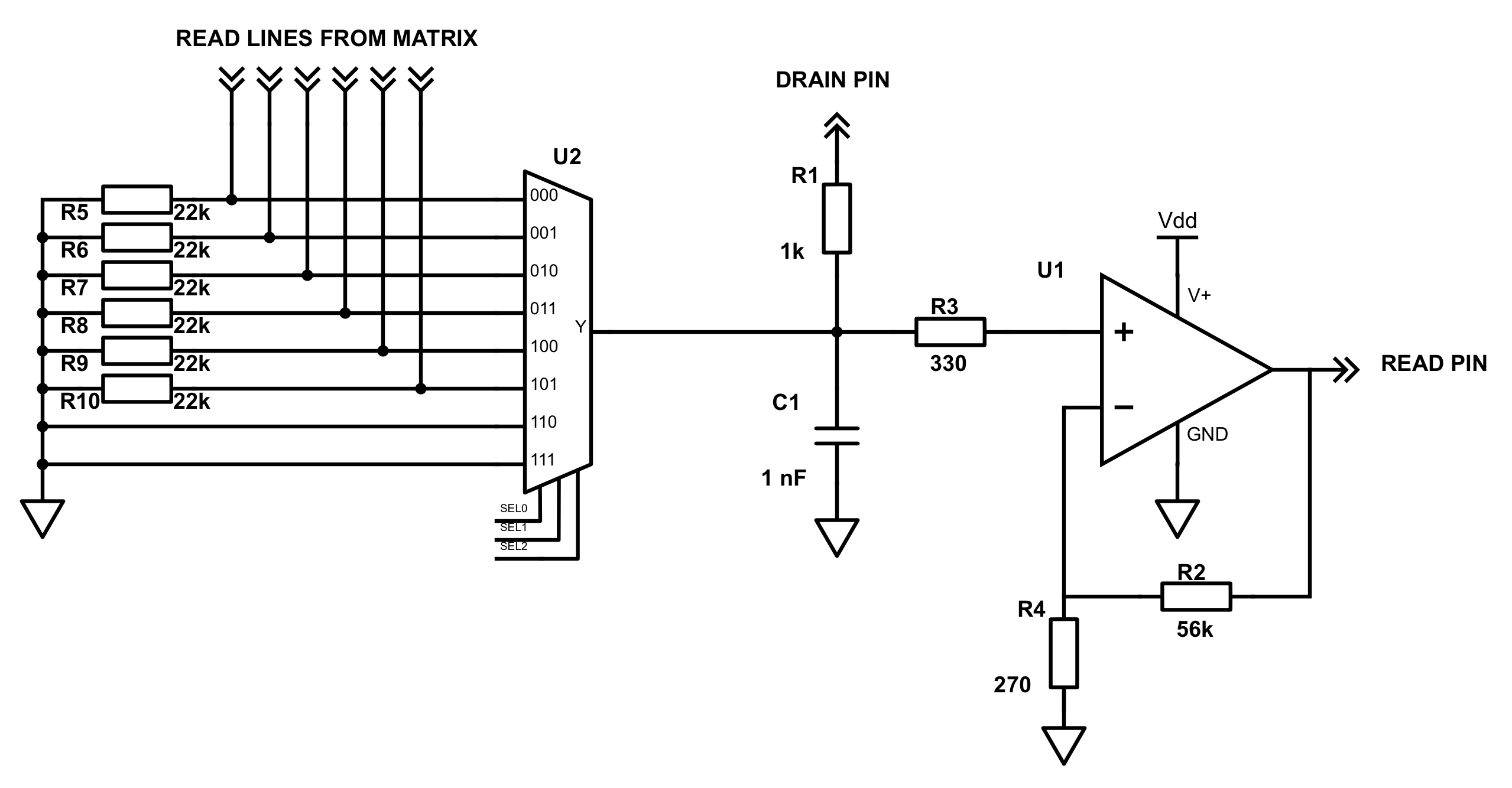
The Frequency of an RC Circuit
For this section, we’ll be focusing on the elements labeled C1, R1, and R3. We can calculate the time constant of our circuit by multiplying our resistance by our capacitance. For simplicity we’ll ignore R1, which we’ll talk about later. This means that our time constant is calculated as:
τ = R3 * C1
  = 22 kΩ * 1 nF
  = 22,000 Ω * 0.000000001 F
  = 0.000022 seconds
  = 22 uS
An RC circuit will reach near-maximum charge, or fully discharge at 5τ. So in our case, that’s 110 microseconds. That may sound good so far, but you have to realize that this is just our discharge time. We haven’t accounted for the ADC read time. Right off the bat, that gives us a scan frequency of at most 100 Hz (not including ADC) for a full sized board. We can help discharge the circuit faster through our drain pin.
Speeding Up Our Resolution
The drain pin is the secret sauce to speed up our RC circuit. While the circuit is charged and the ADC reads, we leave the drain pin floating. This is a state that is not connected, so we can ignore it in our circuit. However, when we need to discharge the circuit, we can pull the drain pin down to ground, reducing the resistance in our circuit (it’s in parallel with the other resistor), speeding up our discharge. Let’s calculate our new resistance:
R = 1 / ( 1 / R1 + 1 / R3 )
  = 1 / ( (1 / 1,000) + (1 / 22,000) )
  = 956 Ω
With our new effective resistance, we can calculate our time constant again:
τ = R * C1
  = 956 Ω * 1 nF
  = 956 Ω * 0.000000001 F
  = 0.000000956 seconds
  = 956 nS
  = 0.956 uS

5τ = 5 * 0.956 uS
   = 4.78 uS
This gives us a far more respectable discharge time. This means that most of the latency in our matrix will be caused by the ADC. We’ll discuss the details of the actual implementation’s latency (including ADC induced latency) when we talk about the software implementation.
Getting Our Voltages Back to Specifications
So there’s a minor problem with our RC circuit. The voltages that come out of it are really small. We can fix that with an operational amplifier (op-amp). By connecting it up a certain way, we can create what is called a “non-inverting op-amp.” What this does is multiply the voltage by a value known as “gain.” We can calculate gain like so:
Gain = 1 + R2 / R4
     = 1 + 56000 / 270
     = 207
This means that we’re multiplying the output voltage by 207. The details of the non-inverting op-amp aren’t super important. Just that its purpose is to multiply the voltage so we can read it with the ADC.
It’s important to note that op-amps can be slow, so we need a fast op-amp to help our frequencies. Smalley’s original guide suggests an OPA350A. I have independently verified that this is a good op-amp that is appropriate for Dopre implementation.
How to Convert to a QMK-style Grid
Dopre works best in a column to row fashion. The details will be covered later, but importantly this means that you need the same “column” pins attached to your grid that you are used to with QMK, but you won’t have any “row” pins. Instead, you’ll have a single “read” pin, several multiplexer selection pins, and a drain pin. The multiplexer selection pins and drain pin can all be any arbitrary GPIO pin. However, the read pin needs to be connected to one of your ADCs, so make sure that your select it appropriately.
Each pad is connected on one side to a column pin, and the other is connected to a row trace. These rows all run back to an analog multiplexer. Each row is connected to a different input channel of the analog multiplexer. Each row is also connected to ground via a 22 kOhm resistor. There is a separate resistor for each row. We then follow the schematic as drawn, connecting all of the pins as labeled.
Final Concerns
R2 and R4 in the circuit use non-standard resistor values. In order to achieve these values, I recommend using a 46k Ohm and a 10k Ohm resistor in series to get R2 and a 470 Ohm and 680 Ohm in parallel to achieve R4.
Conclusion
An RC circuit is a rather simple and elegant solution that we can use to sense capacitance of an ESC keyswitch. It is not suitable to converting Topre to an analog input method, but it is a simple solution that makes QMK implementation easy and relatively cheap. There is still room for improvement and accuracy in this solution, leaving space open to future improvements.
Future Reading
In the future, we’ll talk about the software solution behind Dopre and how it was integrated into QMK. We’ll also talk about the case and PCB implementations of a Dopre solution in a later article.
Sources
-
https://www.keyclack.com/products/bke-topre-dome-replacements ↩
-
https://simple.wikipedia.org/wiki/Switch ↩
-
http://www.realforce.co.jp/en/features/index.html ↩
-
https://arstechnica.com/gadgets/2013/04/from-touch-displays-to-the-surface-a-brief-history-of-touchscreen-technology/ ↩
-
https://blog.codinghorror.com/mouse-dpi-and-usb-polling-rate/ ↩
-
https://www.pubnub.com/blog/how-fast-is-realtime-human-perception-and-technology/ ↩
-
https://electronics-tutorials.ws/rc/rc_1.html ↩